Renvatek Quartz-1 gets a UART and an AXI4-Lite bus (Part 1: the soft IP)
2026-10-23 (updated 2026-11-01)

As you all already know, Renvatek Quartz-1 passed all 39 RISC-V ACT4 compliance tests. That proves the ISA behavior. It does not prove the core can do useful work with the outside world. For that, it needs a peripheral and a way to reach it.
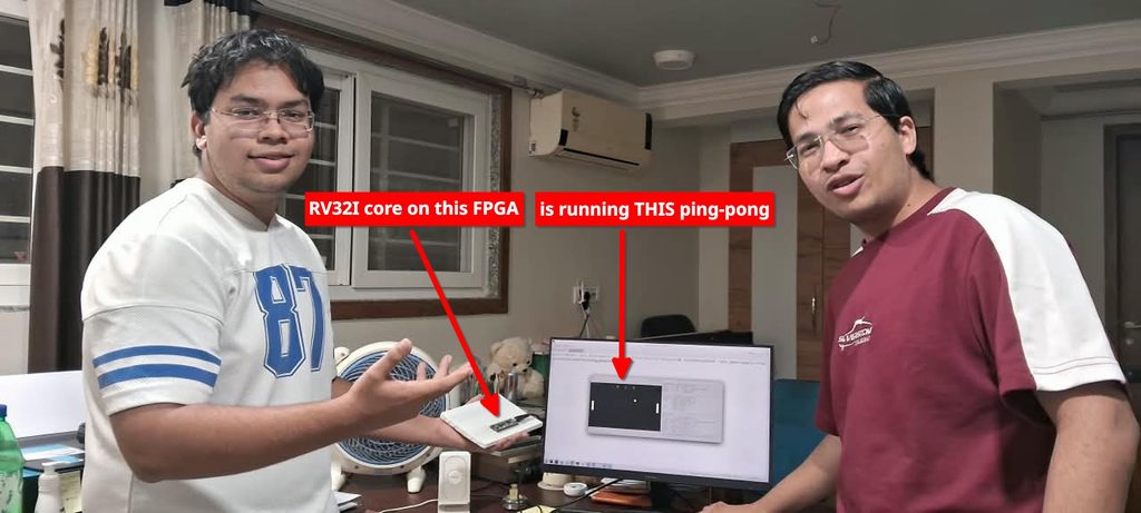
So we split the next step in two. I built the soft IP: the bus and the UART around the core. My twin brother, Prashant, took it onto a real FPGA and wrote the application. This post covers my half. His post picks up where mine ends.
Top-level architecture
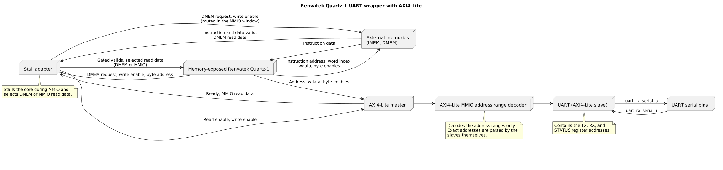
Data flows from the core to the UART through the AXI4-Lite bus:
Core
Renvatek Quartz-1 is a single-hart RV32I core. Its memories are not inside it. I spent a week or so removing my hard-coded RTL memory arrays and exposing real memory ports this time. The module boundary exposes the instruction and data ports. The integrator decides what sits behind them, such as block RAM, an SRAM macro, or a cache.
This keeps the core portable. On an FPGA, the wrapper connects to block RAM. In an ASIC flow, it can connect to something else. The core does not change.
Bus (AXI4-Lite)
Peripherals are reached through memory-mapped I/O. A load or store to an address in the MMIO window becomes an AXI4-Lite transaction. Three blocks handle this:
- AXI4-Lite master: an FSM that turns a core load or store into AXI4-Lite read and write channel handshakes. The FSM concept comes from the eChipHub RTL bootcamp.
- MMIO address range decoder: looks at the address and selects the slave. Right now, there is only one slave, the UART, in the range
0x10000000to0x1000000B. - Stall adapter: The core has no wait state for data accesses. Its only stall input is
imem_valid_i, which holds the PC while low. A second input,dmem_valid_i, enables the register write-back. An AXI4-Lite access takes eight or more cycles, and more when the UART transmitter is busy. When the bridge pulses its ready output, the adapter setscore_imem_valid_ohigh for one cycle, so the PC advances. In that same cycle it setscore_dmem_valid_ohigh, so the load result is written back. The adapter also selects the master’s read data in place of the memory’s read data for that access. Outside the MMIO window, the memory’sdmem_valid_iand read data pass through unchanged.
UART (an AXI4-Lite slave)
The UART peripheral has three registers:
| Address range | Name | Access | Function |
|---|---|---|---|
0x10000000 to 0x10000003 | TXDATA | Write | Queue one byte for transmission. |
0x10000004 to 0x10000007 | RXDATA | Read | Read the last received byte. |
0x10000008 to 0x1000000B | STATUS | Read | Bit 1: TX ready. Bit 0: RX pending. |
lw and sw) to access these registers.The frame format is 8N1: one start bit, eight data bits sent LSB first, no parity, one stop bit. The baud rate and clock frequency are module parameters. In our build, they are 19200 baud and 12 MHz, so one bit lasts 625 clock cycles.
The receiver synchronizes the RX line, detects the start bit’s falling edge, waits half a bit period to confirm it, and then samples each data bit once per bit period. The transmitter is a similar FSM running in the opposite direction. Both are FSMs built from an enum state type and a counter, so they are easy to read in one pass.
To use the UART, software polls STATUS, then reads RXDATA or writes TXDATA. That is the entire programming model.
Why this split works
The core knows only loads and stores. It has no idea a UART exists. Adding a second peripheral means adding a slave and extending the decoder range. The core and the bus master stay untouched.
The ping-pong game uses exactly this path. It is a bare-metal program that polls STATUS, reads a key byte, and writes a reply. No game-specific hardware exists.
What this post does not cover
Prashant’s work covers the clock source, power-on reset, block RAM timing, pin assignment, bitstream build, and the game itself. I wrote the ports and left a note in the top file about what to connect. His post has what he did with them.
Next milestone
The next soft IP is a framebuffer. It will let Renvatek Quartz-1 run graphical apps without a laptop drawing the screen. Today the core sends game state over the UART, and the laptop does all the drawing.
I expect to add the framebuffer as another peripheral on the same AXI4-Lite bus, with its own address range in the decoder. The research on memory size, pixel format, and how the display is driven is on the priority list. I will write about the results once the interface is settled.
Categories: Hardware
Tags: axi4-lite, bus, core, hdl, mmio, renvatek, renvatek-qe001001rv32in0, renvatek-quartz-1, risc-v, rtl, systemverilog, uart
Leave a Reply